Products
- Other Consumer Electronics[1]
- Double-Sided PCB[1]
- Multilayer PCB[10]
- Other PCB & PCBA[10]
- Rigid PCB[7]
Contact Us
- Contact Person : Mr. Lei Jack
- Company Name : Shenzhen Rayming Electronics Co., Ltd.
- Tel : 0086-0755-27348087
- Fax : 0086-0755-27389625
- Address : Guangdong,Shenzhen,RM498 Binye Building Fanghua Road Fuyong Bao'an shenzhen Guangdong China
- Country/Region : China
- Zip : 518103
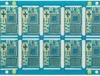
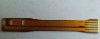
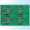
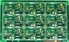
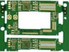
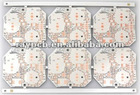
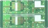
2 Layer Backplane PCB for Telecom


Product Detailed
Related Categories:Other PCB & PCBA
Related Product Searches:2 Layer Backplane PCB for Telecom,High Quality,2-layer Backplane PCB for Telecom, High Frequency PCB,RML51644
Quick-turn prototype and small-quantity PCBs
Base lamination: Teflon
Board thickness: 0.8 mm
PCB layers: 2 layer board
Related Product Searches:2 Layer Backplane PCB for Telecom,High Quality,2-layer Backplane PCB for Telecom, High Frequency PCB,RML51644
2 Layer Backplane PCB for Telecom
Key Product Specifications / Features
Quick-turn prototype and small-quantity PCBs 35um (thickness) copper Base lamination: Teflon Board thickness: 0.8 mm (0.031 inch) Board size: 114.30 x 190.50mm (4.5 x 7.5 inch) PCB layers: 2-layer board Min Conductor width: 0.3 mm (12 mil) Min Conductor spacing: 0.3 mm (12 mil) Min Size of plated through holes: 0.4 mm (16 mil) Min Pad diameter: 0.6mm (24 mil) Working frequency: 1-2G HZ The Surface treatment type: Flash gold Impedance control value: 50OHM +/-10%Selling Point
Fine-line high density quick turn prototype and small volume pcb
Primary Competitive Advantages
Short leading time, Prototype and Small Quantity, multilayer
More detail, welcome to contact me raypcb Lisa skype: raypcb03
2 Layer Backplane PCB for Telecom